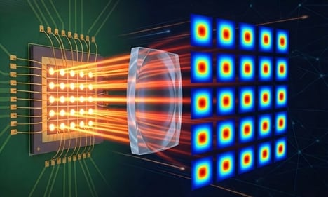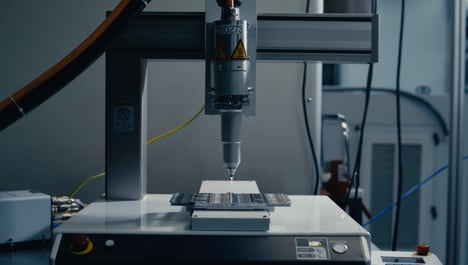


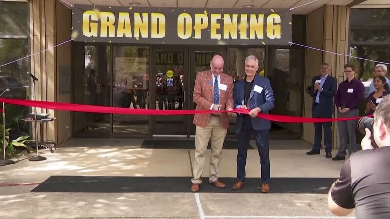
La Luce Cristallina is developing photonic chip materials that let data move with light instead of electrical signals. The Austin startup grows ultra-thin crystal layers on silicon wafers, giving chipmakers a way to build smaller devices that use far less power.
The material traces back to research at the University of Texas and is aimed at the computing load created by artificial intelligence and data centers. Faster chip-to-chip communication can lower energy costs and speed up responses to AI requests.
At a potential 100 times less power, the material could turn photonics from a lab idea into a practical chipmaking input. That would matter most in semiconductor hubs such as Central Texas, where cleaner data transfer and lower electricity use are becoming part of the competitive case for new hardware.
Image Credit: La Luce Cristallina
Why This Trend Is Growing
- Silicon Photonics Integration
- Embedding crystal-grown photonic layers into standard silicon platforms creates openings for lower-power data movement inside next-generation chips.
- AI-efficient Hardware
- Rising AI workloads are expanding demand for components that reduce electricity use while improving chip-to-chip communication speed.
- Crystal-layer Materials
- Ultra-thin crystalline films on wafers introduce new pathways for shrinking devices and making optical data transfer more commercially viable.
Industries Being Reshaped
- Semiconductors
- Chip manufacturers gain a materials-based route to differentiate hardware through faster interconnects and reduced power consumption.
- Data Centers
- Energy-intensive computing facilities face growing potential for infrastructure cost reductions through light-based data transfer technologies.
- Artificial Intelligence
- AI platforms benefit from hardware advances that accelerate response times while easing the power burden of large-scale model processing.