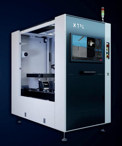

Ultra-precise dispensing is advancing electronics manufacturing by enabling manufacturers to deposit conductive copper paths with micron-level accuracy for semiconductor packaging and advanced printed circuit boards. XTPL's Ultra-Precise Dispensing (UPD) technology is expanding beyond flat panel displays into yield management applications, where precise material placement can reduce defects, improve production yields and support increasingly complex electronic components. The company's latest deployment with a Japanese industrial equipment manufacturer highlights the growing demand for precision dispensing in next-generation electronics production.
For manufacturers, this capability offers a way to improve efficiency while reducing material waste and production losses in high-value semiconductor and PCB fabrication. Expanding into new materials such as copper also broadens the technology's commercial potential across advanced packaging, aerospace, automotive and industrial electronics. As chip architectures become more compact and sophisticated, ultra-precise dispensing platforms could become an increasingly important tool for improving manufacturing quality, scalability and supply chain competitiveness.
Image Credit: XTPL
What's Driving This Trend
- Micron-level Copper Printing
- Conductive copper deposition at micron-scale precision creates new pathways for denser circuit layouts, lower material waste and more flexible semiconductor packaging processes.
- Yield-focused Manufacturing
- Precision material placement is becoming a valuable defect-reduction layer as electronics producers seek higher throughput and stronger economics in advanced fabrication environments.
- Additive Electronics Production
- Selective dispensing of functional materials supports a shift toward additive manufacturing models that can reduce process complexity and enable customized high-performance electronic components.
Who This Affects Most
- Semiconductors
- Advanced chip packaging and compact architectures benefit from ultra-precise conductive path formation that improves manufacturing consistency and supports next-generation device performance.
- Printed Circuit Boards
- High-density PCB fabrication gains commercial potential from fine-line dispensing systems that enable tighter interconnects, reduced scrap and more efficient use of conductive materials.
- Industrial Electronics
- Complex control systems, sensors and embedded electronics are positioned to incorporate precision-printed conductive features that improve reliability across demanding production and operating conditions.